TSMC EDA Alliance, a key component of TSMC Open Innovation Platform®(OIP), reduces design
barriers for customer's adoption of TSMC process technologies. By combining TSMC
and EDA Alliance members R&D capability and resource,
new generations of EDA solutions are enabled to be compliant to TSMC technology requirements. This
helps
customers to better achieve their PPA target in a shorter period of time.
EDA partners in TSMC EDA Alliance offer wide variety of design automation tools that cover all stages
of
IC design needs, ranging from circuit design timing analysis, simulation for design electrical
analysis,
place & route for physical
implementation, and physical layout verification, RC extraction for final design tapeout signoff.
Selected EDA Alliance partners work closely with TSMC's design technology teams to address customer
design needs through the enablement of new EDA tool features that align with TSMC advanced process
development roadmap, as well as the
implementation of TSMC's design methodology in Reference Flows. Through the established work model,
EDA
Alliance partners gain access to TSMC's technical insights to validate their tools and
methodologies.
List of EDA Alliance partners as of 04/22/2026
- Altair Engineering
- Ausdia
- Cadence Design Systems
- iROC Technologies
- Jedat
- Keysight Technologies
- Lorentz Solution
- Primarius
- Siemens EDA
- Silvaco
- SkillCAD
- Synopsys
- Zuken
On top of the TSMC EDA Tool Certification Program, TSMC collaborates with its ecosystem partners to
address the design challenges of new technologies and bring customers solid solutions for design
enablement and turnaround time improvement.
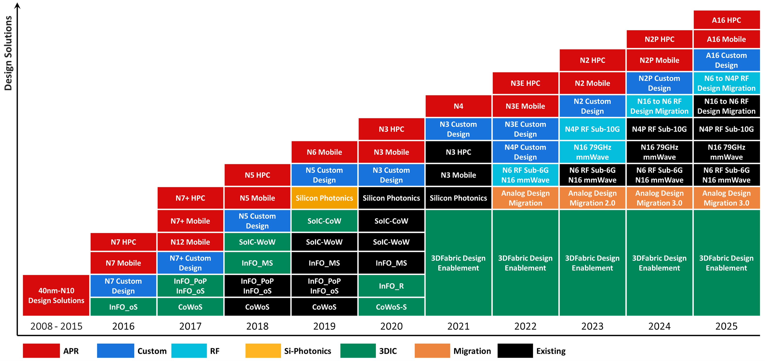
The latest design reference flows are:
A16 Design Reference Flows
Providing comprehensive technology support to address latest GAA design challenges in HPC, mobile and full custom designs. The A16 Mobile and HPC design reference flows enabled synthesis, placement and routing taking full advantage of TSMC GAA methodology for different design applications. The A16 Custom Design Reference Flow offers frontend-to-backend full custom transistor-level design and verification.
TSMC 3DFabric®
Design Enablement Reference Flow
The reference flow aims to use modulization concept realizing 3DIC designs with TSMC
3DFabric®
advanced packaging service. Customers can easily implement their innovative 3DIC designs with the
set of
fundamental building blocks. The required EDA solutions for 3DIC implementation, analysis and
verification are also in place supporting advanced packaging design enablement through the joint
efforts
in certification, and recapped in this reference flow.
Analog Design Migration Reference Flow
Maximizing the reuse of the analog IP blocks. Conventional analog design porting requires manual migration and verification on each design step with tedious and time-consuming operations. To efficiently reuse the proven analog blocks across TSMC technologies, customers can benefit from Analog Design Migration Reference Flow with accelerated processes in schematics migration, layout reuse, and circuit optimization.
RF Design Migration Reference Flow
Leveraging from Analog Design Migration capabilities, the RF Design Migration flow enhances the productivity of migrating the RF designs (N6 to N4PRF) to enjoy the PPA gain in TSMC advanced nodes. The customers can benefit from the RF Migration Flow with accelerated processes in custom passive synthesis & analysis, schematics migration, functional simulations, layout reuse, circuit optimization.
Please login
TSMC-Online
for more information and download.
To better serve our customers with a robust design ecosystem and enable customers’ design with TSMC
latest technology, TSMC has been conducting full-line EDA Tool Certification Program with major
partners
including Cadence, Siemens EDA and Synopsys. The core of the certification program covers the
tool solutions to the latest advanced process technologies (A14, A16, N2P, N3C) and 3DFabric offering.
The advanced process node certifications cover several silicon-centric categories, including physical
implementations (APR for High Density/HPC, Custom Design), timing and power signoffs (STA,
Transistor-level STA), electromigration and IR Drop (Gate-level and transistor-level EMIR), physical
verifications (DRC, LVS, Dummy Fill), RC extractions (RC), simulators, and thermal.
A14 EDA Tool Certification Status
As of 07/10/2026
| A14 Readiness |
Cadence |
Synopsys |
Siemens EDA |
| APR |
|
|
|
| Lib. Characterization |
|
|
|
| Timing |
|
|
|
| Power |
|
|
|
| EMIR |
|
|
|
| DRC |
|
|
|
| Dummy Fill |
|
|
|
| LVS/LPE |
|
|
|
| RC |
|
|
|
| Custom Design |
|
|
|
| Tx EMIR |
|
|
|
| Tx Timing |
|
|
|
| Simulators |
|
|
|
: Certified
: Work in Progress
A16 EDA Tool Certification Status
As of 07/10/2026
| A16 Readiness |
Cadence |
Synopsys |
Siemens EDA |
| APR |
|
|
|
| Lib. Characterization |
|
|
|
| Timing |
|
|
|
| Power |
|
|
|
| EMIR |
|
|
|
| DRC |
|
|
|
| Dummy Fill |
|
|
|
| LVS/LPE |
|
|
|
| RC |
|
|
|
| Custom Design |
|
|
|
| Tx EMIR |
|
|
|
| Tx Timing |
|
|
|
| Simulators |
|
|
|
| Thermal |
|
|
|
: Certified
N2P EDA Tool Certification Status
As of 07/10/2026
| N2P Readiness |
Cadence |
Synopsys |
Siemens EDA |
| APR |
|
|
|
| Lib. Characterization |
|
|
|
| Timing |
|
|
|
| Power |
|
|
|
| EMIR |
|
|
|
| DRC |
|
|
|
| Dummy Fill |
|
|
|
| LVS/LPE |
|
|
|
| RC |
|
|
|
| Custom Design |
|
|
|
| Tx EMIR |
|
|
|
| Tx Timing |
|
|
|
| Simulators |
|
|
|
| PERC |
|
|
|
: Certified
: Work in Progress
N3C EDA Tool Certification Status
As of 07/10/2026
| N3C Readiness |
Cadence |
Synopsys |
Siemens EDA |
| APR |
|
|
|
| Lib. Characterization |
|
|
|
| Timing |
|
|
|
| Power |
|
|
|
| EMIR |
|
|
|
| DRC |
|
|
|
| Dummy Fill |
|
|
|
| LVS/LPE |
|
|
|
| RC |
|
|
|
| Custom Design |
|
|
|
| Tx EMIR |
|
|
|
| Tx Timing |
|
|
|
| Simulators |
|
|
|
| PERC |
|
|
|
: Certified
TSMC 3DFabric®
EDA Tool Certification Status
As of 07/10/2026
: Certified for Technology Requirement